Browse categories
Explore
Fiverr Pro
English
$
USD
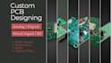
I am an Electronics Engineer specializing in professional PCB design for IoT, embedded, and industrial applications.
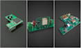
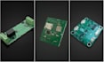
With more than 4 years of experience in electronics design and PCB development, I specialize in embedded systems, IoT hardware, low-power design, product prototyping, and communication modules. I have successfully designed professional and production-ready PCB layouts for a wide range of applications.
What I deliver:
Specialization:
Let's turn your ideas into high-quality, functional PCBs with precision and reliability. Feel free to contact me about your project I will be happy to answer your questions.
Which files will be delivered at the end of project?
Gerber, 3D Step, PDF, BOM and Pick and Place files will be delivered free of cost.
What'd be the PCB Size and Shape?
I will try to make PCB design as small as possible to reduce manufacturing cost. I can also design PCB boards of your custom shapes.
How secure is my design or information?
All your information will be kept confidential, and your intellectual property will stay secure.


