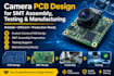
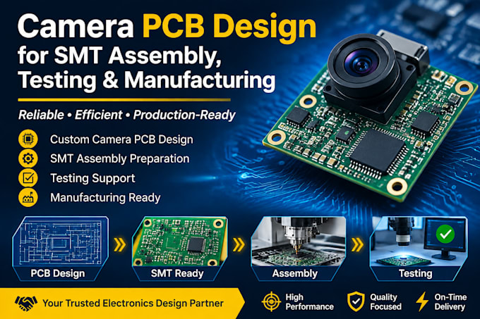
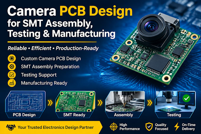
I will design camera pcbs for smt assembly ,testing and production manufacturing

United Kingdom

I speak English, French, German

RF PCB designer

I specialize in PCB layout and electronic design support for RF and microwave circuits, antenna systems, GPS modules, amplifier stages, and audio interfaces. I focus on organized schematics, practical...
About this Gig

Looking for professional camera PCB design and manufacturing preparation? I provide electronic circuit design and PCB development solutions for camera and imaging applications.

My services include:

  • Camera PCB schematic and circuit design
  • Custom camera PCB layout
  • SMT component placement and optimization
  • PCB design for assembly and manufacturing (DFM)
  • Camera sensor and image processing circuit integration
  • Power management and signal routing
  • Connector and interface integration
  • PCB testing and design verification support
  • Prototype development and production preparation
  • SMT assembly planning and manufacturing support

My Development Approach

I focus on developing reliable, compact, and production-ready camera PCB designs while considering component compatibility, electrical performance, assembly requirements, and manufacturing standards.

please Contact me to discuss your camera PCB requirements and the best development approach.

Specialization:

Circuit design

•

Schematics

•

Layout

•

Footprint

•

Gerber

File format:

Gerber

•

STEP

•

BRD

•

SCH

•

PDF

Software:

Allegro

•

Altium Designer

•

Cadence OrCAD

•

Eagle CAD

•

KiCad

Interface:

HDMI

•

MIPI DSI/CSI

•

USB

•

SPI

•

I2C

•

BLE

•

GSM/GPRS

•

LTE