Having issues with your PCB not working as expected?
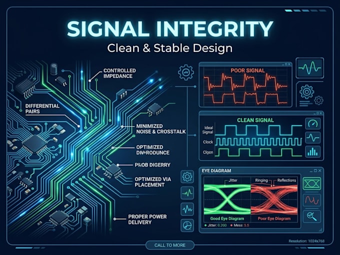
I provide advanced PCB debugging, analysis, and optimization to resolve EMI, signal integrity, noise, and layout problems ensuring your board performs reliably in real-world conditions.
This is not basic editing I apply practical hardware engineering techniques to identify root causes and fix them properly.
Perfect for:
- Hardware startups & engineers
- IoT and embedded systems
- High-speed digital designs
- Analog and mixed-signal circuits
- Boards failing testing or certification
WHAT I FIX
- EMI / EMC issues
- Signal integrity problems (ringing, reflections, crosstalk)
- Grounding and return path issues
- Power integrity and noise
- Poor routing and layout mistakes
- High speed design problems
- Unstable or failing boards
️ WHAT I OFFER
- Full PCB design review and analysis
- EMI/EMC mitigation strategies
- Signal integrity optimization
- Power distribution network (PDN) improvement
- Ground plane and return path correction
- High speed routing fixes (impedance control, length matching)
- Crosstalk and noise reduction
- Stack up optimization (multilayer boards)
- Layout redesign
- Simulation guidance
- Component placement improvement