Browse categories
English
$
USD
Connect to your AI
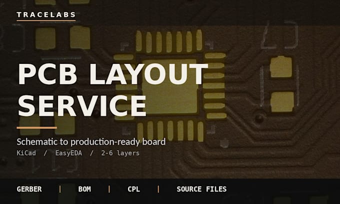
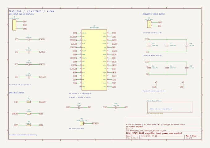
Need a PCB layout service you can trust? I turn your schematic into a clean, production ready board in KiCad, EasyEDA or Altium Designer.
PCB DESIGN AND LAYOUT SERVICES
WHAT YOU RECEIVE
READY FOR JLCPCB AND PCBWAY
Files are checked against fabricator rules, so your order is accepted the first time.
BOARDS I WORK ON
ESP32 and STM32 boards, IoT devices, power supplies, motor drivers and sensor boards.
HOW IT WORKS
1. Send your schematic, board size and constraints.
2. I confirm the scope and start the layout.
3. You review, request changes and get the final files.


File format:
Gerber
•
STEP
•
•
ODB
•
Pcbdoc
Software:
Altium Designer
•
EasyEDA
•
KiCad
•
Proteus
•
AutoCAD
•
PSpice
Interface:
HDMI
•
MIPI DSI/CSI
•
TDM
•
USB
•
PCIe
•
GSM/GPRS
•
LTE
•
CAT-M1
•
NB-IoT
Will I own the source files?
Yes. You receive the full project plus Gerber, BOM and CPL files. The design is yours.
Can you make the board ready for JLCPCB or PCBWay?
Yes. I check the design against their manufacturing rules and prepare the Gerber, BOM and pick and place files so your order passes review.
I don’t have a schematic. Can you help?
Yes, see my gig for schematic and PCB design from an idea. This gig is for boards where you already have the schematic.
Do you sign an NDA?
Yes, on request. Message me before ordering and we can agree it first.
How many revisions are included?
2 in Basic, 3 in Standard and 5 in Premium. You can add more as a gig extra.