Browse categories
Explore
Fiverr Pro
English
$
USD
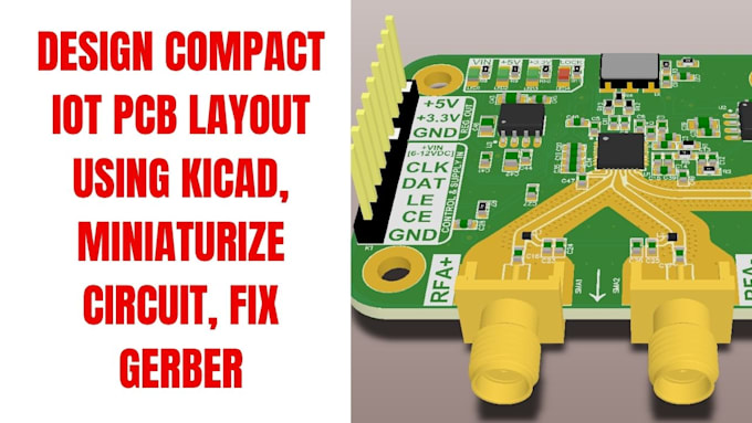
Precision PCB Design That Powers Reliable Innovation
Looking for a professional compact IoT PCB design?
I will design your IoT PCB in KiCad, miniaturize circuits, and fix Gerber files for smooth production.
With years of PCB design experience, I deliver accurate, production-ready layouts that save space, reduce cost, and ensure your project works perfectly. Whether its a prototype, wearable, or smart device, Ill make your PCB compact, optimized, and ready for manufacturing.
What you will get:
Why choose me:
Get your IoT project ready to manufacture today!


What do you need to start?
I need your schematic, component list, and project details.
Can you handle miniaturization?
Yes, I specialize in compact PCB layouts to save space and optimize your design.
Will I get Gerber files ready for production?
Absolutely! All Gerber files are verified and production-ready.
Can you fix errors in existing PCB designs?
Yes, I can troubleshoot and correct Gerber or layout issues efficiently.
What if my project is complex?
No problem! I handle simple to advanced IoT PCB designs and provide professional solutions.