Browse categories
Explore
Fiverr Pro
English
$
USD
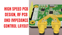
Precision PCB Design That Powers Reliable Innovation
Need a high-speed or RF PCB that performs without signal issues?
I specialize in high-speed PCB layout, RF PCB, and impedance control routing to ensure clean signals, minimal noise, and reliable performance for your project.
Whether you're working on communication systems, IoT devices, or high-frequency circuits, I provide production-ready boards built with proper stackup, trace control, and signal integrity in mind.
What I Offer
Why Choose Me
Turn your idea into a high-performance PCB
Message me before ordering!


Do you handle RF and high-frequency boards?
Yes, I specialize in RF layouts and high-speed circuits.
Will impedance be controlled properly?
Yes, I calculate and apply proper trace width and stackup.
What files will I receive?
Gerber files, source files, schematic, and BOM.
Can you fix or improve an existing PCB?
Yes, I can optimize or redesign existing layouts.
Do you support manufacturing?
Yes, files are ready for PCB manufacturers.


