Browse categories
Explore
Fiverr Pro
English
$
USD
Electronic engineering, Embedded systems designer, Arduino programming
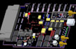
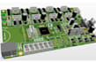
I am a professional PCB layout designer with hands on experience designing production ready PCBs for startups, IoT products, and manufacturers. I focus on clean routing, manufacturability, and signal integrity, ensuring your board works right the first time.
I provide professional PCB layout design from your schematic or concept, optimized for manufacturing, assembly, and performance.
What I Offer;
PCB layout from schematic
Multilayer PCB design 212 layers
SMT & THT component placement
DRC clean, fabrication ready files
Gerber, BOM, Pick & Place
Manufacturer friendly design JLCPCB, PCBWay, etc.
Best For;
Startups & hardware founders
Engineers outsourcing layout
Prototypes & production boards
Used For;
IoT devices
Consumer electronics
Industrial control boards
Embedded systems
Why Choose Me;
Focus on DFM & DFA
Clean, readable routing
Fast communication
100% manual design no auto route
On time delivery
NOTE; Message me before ordering to review your requirements and get the best results.

What do you need to start the PCB layout?
I need your schematic file (PDF or CAD), board size, layer count, and manufacturing requirements. If you don’t have everything ready, you can message me and I will guide you.
Will the PCB be ready for manufacturing?
Yes. All PCB layouts are DFM and DFA optimized and delivered with Gerber files, BOM, and Pick & Place, ready for fabrication and assembly.
Which PCB software do you use?
I use industry-standard PCB design tools suitable for professional and production-level PCB layout.
Can you design multilayer or SMT PCBs?
Yes. I design 2–12 layer PCBs, including SMT and THT designs, optimized for performance and manufacturability.
Do you support PCB manufacturers like JLCPCB or PCBWay?
Yes. I fully support JLCPCB, PCBWay, Seeed, and other manufacturers, and can adapt the design to their requirements.


