Browse categories
Explore
Fiverr Pro
English
$
USD
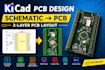
PCB Designer KiCad 2 Layer and 4 Layer PCB Design
Need to turn your schematic into a clean and professional PCB layout?
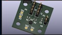
HI! I'm Manoj and I will convert your schematic into a professional 2-layer PCB layout using KiCad, ready for manufacturing.
What I can do for you:
What you will receive:
Clean and organized PCB layout
Proper component placement and routing
DRC-checked design
Gerber files for manufacturing
BOM when required
Editable KiCad source files
Why choose my service?
I focus on clean PCB layouts, proper routing, manufacturability, and clear project files. I will work according to your schematic and requirements and keep you updated throughout the process.
Please contact me before ordering if your PCB has special requirements or you are unsure which package to choose.
Let's turn your schematic into a functional PCB!


File format:
Gerber
•
SCH
•
3DS
•
•
Pcbdoc
Software:
KiCad
•
Matlab
Interface:
I2S
•
UART
•
SPI
•
I2C


