Browse categories
English
$
USD
Connect to your AI
Electronics and Embedded Systems Engineer
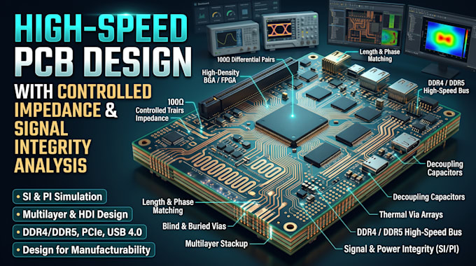
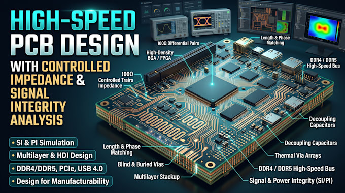
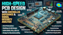
High-speed signals can fail even when a PCB passes basic design-rule checks. Incorrect trace geometry, impedance mismatches, poorly routed differential pairs, and unsuitable stackups can cause reflections, timing errors, crosstalk, and unreliable interfaces
I design high-speed PCBs with controlled impedance and signal integrity in mind, helping turn demanding electrical requirements into practical, manufacturable board layouts.
My services include:
What I will provide:
PCB layout, impedance control, SI review, and fabrication files.
Why choose me:
Precision routing, practical engineering, and production-focused design.
Send your schematic, interface requirements, target impedance, and available stackup details. Let's develop a reliable high-speed PCB tailored to your project.
File format:
Gerber
•
STEP
•
VRML
•
BRD
•
SCH
Software:
Allegro
•
Altium Designer
•
KiCad
•
Arduino
Interface:
HDMI
•
MIPI DSI/CSI
•
PCIe
•
Wi-Fi
•
BLE
•
BT
•
GSM/GPRS
•
LTE
•
NB-IoT