Browse categories
Explore
Fiverr Pro
English
$
USD
I design high performance RF PCB layouts for 5G, IoT, and mmWave systems
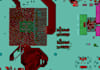
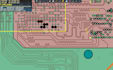
I will design high-speed PCB layouts with optimized signal integrity, impedance control, and power integrity for reliable performance in modern electronic systems. My service is ideal for high-data-rate applications such as PCIe, USB, DDR, HDMI, and Ethernet.
What I offer:
High-speed multilayer PCB layout
Controlled impedance routing and stack-up design
Signal integrity (SI) and power integrity (PI) optimization
Differential pair routing (PCIe, USB, DDR, Ethernet)
Crosstalk, noise, and EMI reduction
Design for Manufacturing (DFM) support
Why choose me:
Strong expertise in high-speed and RF PCB design
Clean, optimized, and production-ready layouts
Focus on real-world performance and reliability
Fast communication and on-time delivery
Software I use:
Altium Designer, Cadence OrCAD, Allegro, KiCad, LTspice, PSpice
Files delivered:
Gerber files, ODB++, BOM, pick-and-place, schematic files, stack-up details, fabrication drawings, and design reports
Contact me before placing an order to discuss your project requirements and get a high-performance PCB design tailored to your needs.

What do you need to start my high-speed PCB project?
I need your schematic (if available), design requirements, layer count, stack-up preferences, and interface details (PCIe, USB, DDR, etc.).
Do you ensure controlled impedance in your designs?
Yes, I design all high-speed traces with proper impedance control based on stack-up and manufacturer specifications.
. Can you handle signal integrity and power integrity analysis?
Yes, I perform SI/PI optimization to minimize noise, crosstalk, and signal loss.
What types of high-speed interfaces do you support?
I work with PCIe, USB, HDMI, DDR, Ethernet, and other high-speed communication interfaces.
What software do you use for PCB design?
I use Altium Designer, Cadence OrCAD/Allegro, KiCad, LTspice, and PSpice.


