Browse categories
Explore
Fiverr Pro
English
$
USD
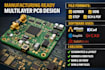
Hi, Im Daniel, a professional PCB designer specializing in manufacturing-ready multilayer PCB design with DFM optimization, ensuring your boards are fabrication and assembly ready.
I deliver:
I use Altium Designer, KiCad, EasyEDA, Cadence OrCAD, SolidWorks for high-speed, RF, IoT, and embedded system boards.
Why choose me? I ensure production-ready, error-free PCB, fully compliant with industry standards.
Message me now to turn your concept into a reliable, ready-to-manufacture PCB!

Can you design multilayer PCBs for high-speed or RF applications?
Yes! I specialize in high-speed, RF, and IoT PCB design, including controlled impedance, signal integrity, and EMI reduction to ensure your boards perform perfectly.
What file formats and software do you provide?
I deliver Gerber, ODB, SCH, PDF, and STEP files. I work with Altium Designer, KiCad, EasyEDA, Cadence OrCAD, and SolidWorks for professional manufacturing-ready designs.
do you provide manufacturing-ready PCBs and DFM checks?
Absolutely! Every design includes DFM review, stackup planning, BOM, pick-and-place files, and all fabrication-ready documents for seamless production.


