Browse categories
Explore
Fiverr Pro
English
$
USD
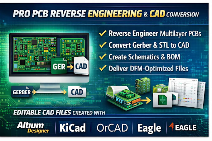
Hi, Im Daniel, a professional PCB designer. I specialize in PCB reverse engineering and Gerber to editable CAD conversion, ensuring your boards are fully reconstructible and manufacturing-ready.
What I deliver:
I focus on signal integrity, multilayer reconstruction, DFM optimization, and accurate PCB cloning. My work ensures your design works flawlessly and is ready for prototyping or production.
Lets turn your PCB concept, Gerber, or STL files into high-quality, editable CAD files quickly and precisely.
Message me now to get your project started!


Can you reverse engineer multilayer PCBs?
Yes! I can reverse engineer single, double, and multilayer PCBs, delivering accurate schematics, Gerber, and editable CAD files.
Which file formats will I receive?
You will get Gerber, SCH, BRD, ODB, STEP, and optional PDF for verification. Files are compatible with Altium, KiCad, Eagle, OrCAD, and Fusion 360.
How fast can you deliver the project?
Delivery depends on complexity: Basic 1–2 layer PCBs in 1–3 days, multilayer or STL-to-STEP projects 3–7 days. Fast delivery options are available.