Browse categories
Explore
Fiverr Pro
English
$
USD
HELLO AND WELCOME!
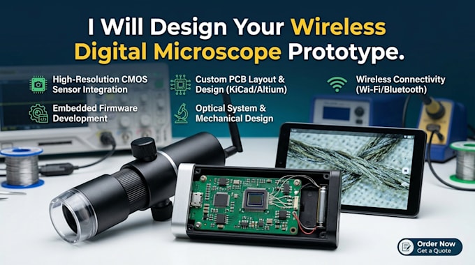
Building a high-quality wireless digital microscope requires precise integration of optics, CMOS imaging technology, embedded electronics, and RF communication. From image sensor interfacing and high-speed signal routing to low-noise power design and wireless data transmission, every hardware component must be engineered for reliable image capture and stable performance.
What I Will Provide;
Why Choose Me?
Have a concept for a wireless digital microscope? Contact me before placing your order. MESSAGE NOW AND LET'S GET STARTED!!!!!!!!

Specialization:
Circuit design
•
Schematics
•
Footprint
•
Gerber
File format:
Gerber
•
STEP
•
3DS
•
Software:
Allegro
•
Eagle CAD
•
KiCad
•
AutoCAD
Interface:
HDMI
•
USB
•
I2C
•
Wi-Fi
•
BLE
•
BT
•
LTE
What types of wireless digital microscopes can you design?
I design portable, handheld, laboratory, industrial inspection, medical, educational, and custom wireless digital microscope prototypes.
Can you integrate WiFi for wireless image transmission?
Yes. I can design hardware with WiFi (and Bluetooth if needed) for live image streaming, remote monitoring, and mobile connectivity.
Which processors can you use?
I support ESP32, STM32, Raspberry Pi Compute Module, NXP, and other embedded processors depending on your project needs.
Can you prepare the design for PCB fabrication and assembly?
Absolutely. All designs follow DFM/DFA best practices and are optimized for prototype and mass production.