Browse categories
Explore
Fiverr Pro
English
$
USD
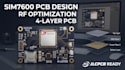
SIM7600 PCB Layout with RF Optimization and 4 Layer Design
A reliable cellular PCB requires more than placing a modem and connecting traces. RF routing, grounding, stackup selection, power delivery and antenna integration must work together to support stable LTE performance.
I develop SIM7600 PCB layouts focused on RF optimization, compact embedded electronics and JLCPCB manufacturing requirements. Whether you need a simple modem board or a complete 4 layer cellular platform, I can help turn your circuit concept into a structured and production ready PCB design.
What I offer:
Why choose me:
I focus on practical RF layout, signal integrity, manufacturability and clean engineering documentation.
What you will get:
Message me with your schematic, module datasheet and board requirements

Can you design a 4 layer SIM7600 PCB?
Yes. I can create a 4 layer stackup with dedicated ground planning, controlled RF routing and optimized power distribution.
Do you handle SIM7600 RF and antenna routing?
Yes. I can route the RF path, create antenna connection areas and include matching network footprints based on the module reference design.
you prepare the PCB for JLCPCB manufacturing?
Yes. I can prepare Gerber, drill, BOM and pick-and-place files according to the required manufacturing specifications.
Do you work with KiCad?
Yes. I can develop the schematic and PCB layout using KiCad, depending on your project requirements.
What do you need to start?
Please provide the SIM7600 module datasheet, schematic, board dimensions, layer preference, antenna requirements and manufacturing details.
