Browse categories
Explore
Fiverr Pro
English
$
USD
Embedded Systems and Multilayer PCB Engineer for Arduino ESP32 STM32 IoT Devices
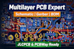
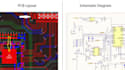
Design Multilayer PCB, Schematic, Gerber, BOM for JLCPCB PCBWay Manufacturing Fast & Reliable
I will engineer and develop high quality schematic diagrams, multilayer PCB layouts, Gerber files, and BOM ready for JLCPCB and PCBWay manufacturing. I focus on clean routing, strong signal integrity, and production ready standards to ensure reliable performance. Whether you need simple boards or complex multilayer PCBs, I deliver accurate, optimized solutions tailored to your project. Get efficient, error free files that ensure smooth fabrication and professional results for your electronic systems.
What Youll Get:
Why Choose Me:
Contact me now to get your PCB professionally engineered and ready for production!
What do you need to start my PCB design?
I need your project details, circuit idea, board size, layer count, and components list.
Will my files be ready for JLCPCB and PCBWay?
Yes, all files are fully compatible and ready for manufacturing on both platforms.
Can you design multilayer PCBs?
Yes, I design up to 6-layer PCBs with proper routing and optimization.
What files will I receive?
You will get schematic, PCB layout, Gerber files, BOM, and Pick & Place files.
Do you offer revisions?
Yes, revisions are included based on your selected package to meet your needs.


