Browse categories
Explore
Fiverr Pro
English
$
USD
Embedded Systems and Multilayer PCB Engineer for Arduino ESP32 STM32 IoT Devices
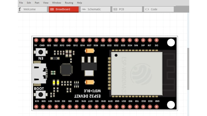
Need precise Multilayer PCB Layout Routing and a clean Fritzing Diagram for your Arduino, ESP32, or STM32 project? That's my specialty.
I handle the full multilayer PCB routing process signal layers, power planes, differential pairs, and impedance control plus clear Fritzing diagrams for documentation and prototyping.
ROUTING & LAYOUT SERVICES:
DELIVERED FILES:
Clean routing is what separates a board that works from one that fails at 1000Hz.
Message me your schematic and let's route it right!
What is PCB routing and why does it matter?
PCB routing is the process of drawing copper traces that connect components according to the schematic netlist. Good routing prevents signal interference, ensures proper power delivery, and avoids EMI issues. Bad routing causes boards to fail intermittently or not work at all especially at higher
Can you do impedance controlled routing for high speed signals?
Yes. I calculate trace widths for 50Ω, 90Ω, and 100Ω differential pair impedance using your PCB stackup parameters. This is essential for USB, HDMI, Ethernet, RF, and high-speed memory interfaces. I provide the stackup spec for your manufacturer.
Do you handle differential pair routing for USB and SPI?
Yes. I route differential pairs (D+/D- for USB, SDIO, LVDS) with matched trace lengths, consistent spacing, and proper reference plane continuity. Length-matching tolerance and via placement follow IPC-2141 guidelines for your target frequency.
What is via stitching and do I need it?
Via stitching connects ground planes across layers using a grid of small vias, reducing ground impedance and improving EMI shielding. I recommend it for RF designs and high-current power sections.
Can you route a PCB from my existing KiCad schematic?
Yes. Share your KiCad schematic (.kicad_sch) and I'll handle the complete PCB layout — component placement, copper pour setup, trace routing, DRC cleanup, and Gerber export. I can also suggest schematic improvements before routing begins.
How do you handle power planes in multilayer PCBs?
Internal power and ground planes in 4+ layer boards are implemented as solid copper pours on dedicated layers. I split planes correctly for different voltage domains, add thermal reliefs for through-hole pads, and ensure plane stitching vias are placed for continuous reference planes.
Do you route boards with both digital and analog sections?
Yes. Mixed-signal PCB layout requires careful partitioning separate analog and digital ground zones, star-point ground connections, guard traces around sensitive analog inputs, and controlled return current paths. I apply these practices to prevent noise coupling between domains.