Browse categories
Explore
Fiverr Pro
English
$
USD
PCB Designer Circuit Boards, Schematics and KiCad Layouts
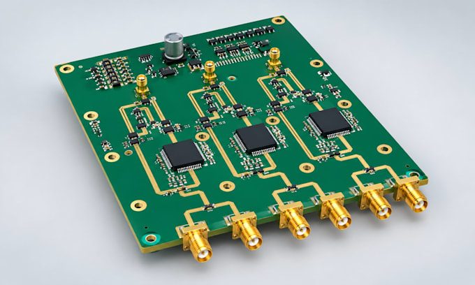
I provide professional PCB design and layout services for electronics projects, from simple circuits to complex multilayer boards. I can help with schematic design, PCB routing, component placement, and preparation of manufacturing-ready files using KiCad, EasyEDA, or other supported PCB design software.
WHAT YOU WILL GET
WHY CHOOSE ME
I focus on accuracy, quality, and clear communication. My goal is to deliver a reliable PCB design that meets your specifications, follows applicable design rules, and is ready for manufacturing. I pay attention to detail and work with you to achieve the best results for your project.
DELIVERABLES
Please contact me before placing an order to discuss your requirements
What information do you need to start my PCB design?
Please provide your project requirements, schematic (if available), component list, board dimensions, preferred software, and any specific design constraints.
Can you design a PCB from scratch?
Yes, I can assist with schematic design and PCB layout based on your project requirements. Please contact me to discuss the complexity of your circuit.
Which PCB design software do you use?
I can work with supported PCB design tools such as KiCad, EasyEDA, or other agreed software, depending on your project requirements.
Will I receive manufacturing-ready files?
Yes, if included in your selected package, I can provide Gerber files, drill files, and other required manufacturing outputs after design rule checks.
Do you provide the PCB source files?
Yes, editable project files are included according to the selected package, allowing you to review or modify the design later.
