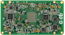
I will design 4 layer and multilayer pcb layout from schematic using diptrace

United Kingdom

I speak English, Spanish, French, German

pcb power expert

Hello, I am an Embedded Systems and Power Electronics Engineer specializing in EMC/EMI troubleshooting, industrial PCB design, and high-performance electronic systems. I help startups and companies d...
About this Gig

Struggling to convert your schematic into a compact 4-layer PCB? Moving from 2-layer to multilayer PCB requires proper stackup planning, routing strategy, and power integrity.


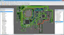
I will help you with a clean, optimized, and production-ready multilayer PCB using DipTrace

I am an experienced PCB Engineer specializing in multilayer PCB layout, high-density routing, and compact board design. I ensure your PCB is efficient, manufacturable, and meets real world performance requirements.


What I Offer

  • 4-layer and multilayer PCB layout
  • Schematic to PCB conversion
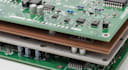
  • PCB stackup design (signal, power, ground planes)
  • High-density routing optimization
  • Power and ground plane
  • PCB size reduction and optimization
  • Design for Manufacturability (DFM)


 Why Choose Me?

  • Clean and optimized PCB layout
  • Proper layer stackup and routing strategy
  • Reduced noise and improved performance
  • Manufacturing ready de-sign


Please send your schematic, board size constraints, layer requirements, and any reference design so I can deliver the best result.
Specialization:

Circuit design

Schematics

Layout

Simulations

File format:

Gerber

STEP

VRML

SCH

PDF

Software:

Allegro

Altium Designer

DipTrace

Eagle CAD

EasyEDA

Interface:

HDMI

MIPI DSI/CSI

I2S

UART

USB

SPI

SDIO

Wi-Fi

BT

GSM/GPRS

LTE