Browse categories
Explore
Fiverr Pro
English
$
USD
Are you struggling to turn your electronic idea into a working circuit?
Many developers face incorrect schematics, messy PCB layouts, signal noise, routing issues, and designs that cannot be manufactured properly.
These problems lead to failed prototypes, wasted time, and higher costs.
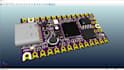
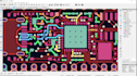
I will solve this by designing professional KiCad PCBs and accurate schematics with optimized layouts and manufacturing-ready Gerber files.
I focus on clean, reliable, and efficient designs ready for real-world production.
What I design:
Benefits:
Files delivered:
Lets turn your idea into a professional and manufacturing-ready PCB design.
Send me a message now and lets start building your project today.

Do you offer revisions if changes are needed?
Yes, I provide revisions to ensure your PCB meets your exact requirements.
Can you work on complex or multi-layer PCB designs?
Yes, I can design both simple and advanced multi-layer PCB systems.
Will I get manufacturing-ready files?
Yes, I provide Gerber files, drill files, BOM, and Pick & Place files for production.
Can you design both schematic and PCB layout?
Yes, I design complete KiCad schematics and PCB layouts with professional routing.
What do you need to start the PCB and schematic design?
I need your circuit idea, requirements, reference design, or component list.


