Browse categories
Explore
Fiverr Pro
English
$
USD
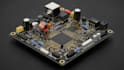
Wireless PCB Designs That Perform in the Real World
Wireless PCBs need more than just connections they need the right layout to perform reliably. I design multilayer PCBs with Wi-Fi, Bluetooth, and RF that are optimized for performance, manufacturability, and stability.
Using tools like Altium Designer, Eagle, Fusion 360, and EasyEDA, I create clean schematics and layouts for 212 layer boards, including RF and impedance-controlled designs.
What I Offer:
Message me to discuss your wireless PCB project.

Specialization:
Circuit design
•
Schematics
•
Layout
•
Footprint
File format:
Gerber
•
STEP
•
VRML
•
SCH
•
Software:
Altium Designer
•
Eagle CAD
•
EasyEDA
•
Fusion 360
•
KiCad
•
Matlab
Interface:
MIPI DSI/CSI
•
I2S
•
UART
•
USB
•
SPI
•
I2C
•
PCIe
•
Wi-Fi
•
BLE
Can you design PCBs using Wi-Fi, Bluetooth, or RF modules instead of chip-down designs?
Yes. I can work with both pre-certified wireless modules and chip-level RF designs, depending on your project requirements and certification needs.


