Browse categories
Explore
Fiverr Pro
English
$
USD
ESP32 IoT and Flexible PCB Design Expert, KiCad, Altium, DFM for JLCPCB
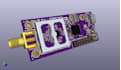
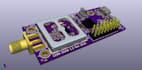
Design RF high speed multilayer PCB impedance control antenna layout in KiCad
Struggling with signal integrity issues, EMI, or failed RF boards at JLCPCB? I deliver professional high-speed and RF PCB designs with precise impedance control, antenna routing, and DFM-checked files that work on the first order perfect for 5G modules, Wi-Fi/BLE devices, IoT sensors, or wireless wearables.
WHAT YOU GET:
WHY CHOOSE ME:
WHAT I NEED FROM YOU:
Ready to get your RF or high-speed PCB manufactured without respins? Message me your project details


What software do you use?
KiCad (primary), Altium & EasyEDA available.
Are files JLCPCB/PCBWay ready?
Yes, full DFM and impedance control for direct upload.
Do you support RF or 5G designs?
Yes, this is my top specialty.
Which interfaces do you support?
Wi-Fi, BLE, BT, Ethernet, USB, SPI, I2C, CAN, SDIO, MIPI and more.
Do you do antenna design?
Yes, routing, matching and tuning included.
What exact files do I receive?
Gerber, Drill, BOM (Excel), Pick & Place, 3D STEP, PDF schematic & source files.
Can you handle high-speed or signal integrity?
Yes, full impedance control and simulation when needed.


