Browse categories
Explore
Fiverr Pro
English
$
USD
United States
Advanced PCB Design for RF, High Speed, HDI and Wireless Electronics
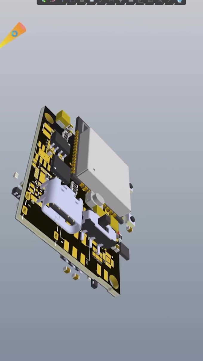
Have a PCB that is too dense, too small, difficult to route, or constrained by BGA, microvias, flex, RF, or high-speed signals? I design HDI, rigid-flex, RF and high-speed PCBs to turn complex layouts into organized, fabrication-ready boards.
What I Offer;
Software Used;
Deliverables;
Suitable For;
Wireless devices
Compact electronics
Wearables
IoT, medical, industrial and other space-constrained hardware using PCIe, USB, Ethernet, HDMI, MIPI, Wi-Fi, BLE, LTE and similar interfaces.
What I Need;
Your schematic/BOM, board size, components, layer requirements, stackup, mechanical constraints and manufacturer specifications.
Have a complex board? Send the details before ordering so I can confirm the scope.


What type of PCB projects can you handle?
I can work on HDI, rigid-flex, flex circuit, RF, high-speed, multilayer, BGA, microvia, fine-pitch, compact and miniature PCB projects.
Can you handle BGA and microvia routing?
Yes. I can handle BGA escape routing, fine-pitch components, microvia structures and high-density routing. Please provide the BGA dimensions, pitch, layer stackup and manufacturer requirements when available.
Can you design rigid-flex and flexible PCBs?
Yes. I can design rigid-flex and flex circuit layouts for compact or space-constrained electronics. Mechanical dimensions, bend areas, layer construction and fabrication requirements are needed for accurate work.
Can you work with RF and high-speed interfaces?
Yes. Projects can include RF, wireless and high-speed interfaces such as PCIe, USB, Ethernet, HDMI, MIPI, Wi-Fi, BLE and LTE. Signal routing and impedance requirements should be provided when available.
What files will I receive?
You can receive Gerber, ODB, STEP/VRML, PDF, schematic, BOM, 3D model, fabrication-ready files and source files.
What do you need from me before starting?
Please provide your schematic, BOM, board dimensions, component data, layer requirements, stackup, mechanical constraints and manufacturer specifications. Existing PCB files are also helpful for redesign or layout work.