Browse categories
Explore
Fiverr Pro
English
$
USD
PCB design, firmware, embedded system engineering for IoT, RF, power electronics
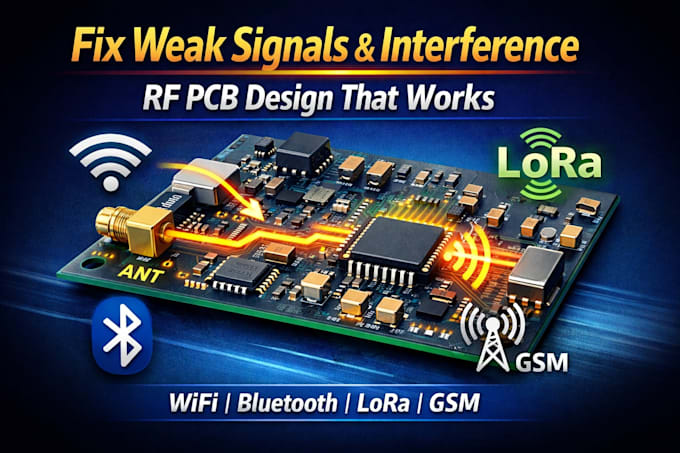
I design RF PCBs that solve real-world wireless issues like weak signal, instability, and interference in WiFi, Bluetooth, LoRa, and GSM systems.
Whether you're building an IoT device or RF module, I ensure your design works reliably in real-world conditions not just in theory.
If your project involves Wi-Fi, Bluetooth, LoRa, GSM, LTE, or other RF systems, proper layout and impedance control are critical. Poor return paths, incorrect stackups, or bad grounding can cause signal loss, unstable connections, and failed performance.
What I focus on:
What you will receive:
Applications I work on:
Contact me before ordering to review your project...


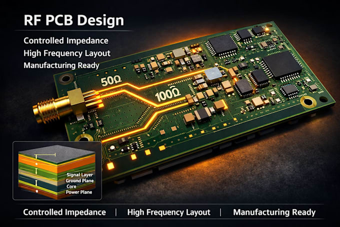
Do you calculate controlled impedance values?
Yes. I design based on required impedance (e.g., 50Ω, 90Ω differential, 100Ω differential). Final trace width depends on your PCB manufacturer’s stackup. For Premium projects, I assist in defining stackup parameters.
Do you design RF antennas?
I can design PCB antennas and provide layout guidance. However, precise antenna tuning and certification testing require lab validation and VNA measurements after fabrication
Do you guarantee RF performance?
No one can guarantee RF performance without physical testing. I follow best-practice RF layout rules to minimize risk, but real-world validation is always required.
Do you handle GHz designs?
Yes, but complexity and layer count affect pricing. High-frequency (>1GHz) boards require stricter stackup control and layout discipline.
Will you contact my PCB manufacturer?
I can provide fabrication-ready files and impedance targets. Direct coordination with the manufacturer is available in Premium only.
What do you need before starting?
Target frequency • PCB stackup (if available) • Impedance requirements • RF chipset/module details • Board size constraints