Browse categories
Explore
Fiverr Pro
English
$
USD
professional pcb designer and Electrical Engineering
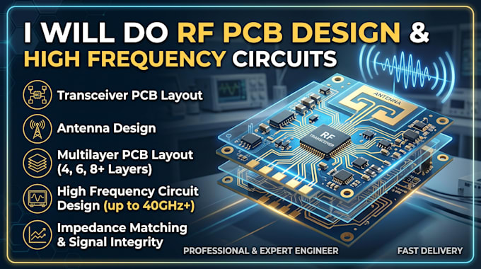
I Will Do RF PCB Design, Transceiver PCB Layout, Antenna, Multilayer PCB Layout & High Frequency Circuit Design
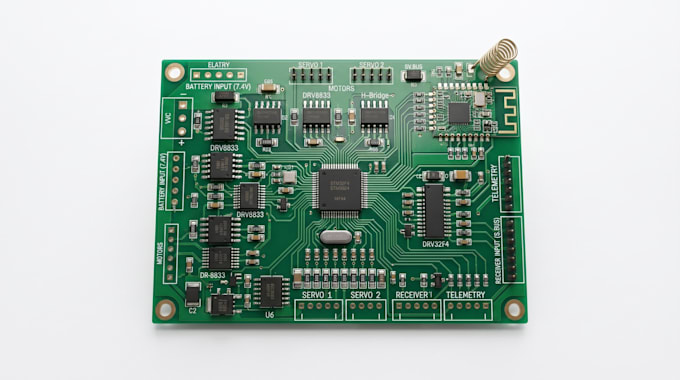
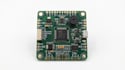
I specialize in RF PCB design, transceiver PCB layout, antenna integration, and multilayer high-frequency PCB development for modern electronic products. Whether you need a compact wireless board, RF module, or high-speed circuit, I will deliver a clean, optimized, and manufacturing-ready PCB to your requirements.
My Services Include
RF & Wireless Technologies
️
You Will Receive
Contact me before placing an order
What PCB design software do you use?
I work with Altium Designer, KiCad, Eagle CAD, and EasyEDA depending on your project requirements.
Can you design multilayer and high-frequency RF PCBs?
Yes, I specialize in multilayer RF PCB layouts, impedance-controlled routing, antenna integration, and high-frequency circuit design.
Do I need to provide a schematic?
Yes, preferably, but if you only have an idea or rough concept, I can also help create or improve the schematic.
Will I receive manufacturing-ready files?
Yes, you will receive Gerber files, drill files, BOM, pick-and-place files, and other files required for PCB manufacturing.
Can you help with antenna and RF matching circuits
Yes, I can design PCB antennas, RF matching networks, and optimize layouts for better RF performance.
Do you support IoT and wireless communication projects?
Absolutely, I work on WiFi, Bluetooth, LoRa, GSM, GPS, Zigbee, and other wireless IoT systems.
How long does the PCB design process take?
Delivery time depends on project complexity, but small projects can be completed within a few days while advanced RF designs may take longer.
Can you redesign or improve an existing PCB?
Yes, I can optimize, redesign, or troubleshoot existing PCB layouts to improve performance and manufacturability.