Browse categories
Explore
Fiverr Pro
English
$
USD
Power Electronics PCB Designer SMPS, BMS, Inverters and DC DC
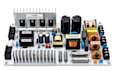
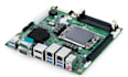
Need a PCB for high-current applications or advanced power electronics? I provide PCB design and optimization for high-current circuits and GaN/SiC power stages, focusing on current paths, thermal behavior, and manufacturability.
My services include:
I help reduce losses, improve heat distribution, and create practical layouts for your requirements. Deliverables may include editable design files, Gerbers, drill files, a bill of materials, pick-and-place data.
To start, share your schematic or PCB files, target voltage and current, board dimensions, key components, and manufacturing constraints. I will review the requirements and confirm the scope before work begins.
Whether you need a new power PCB layout or improvements to an existing design, I provide communication and organized files for review and production preparation.
Please message me before ordering to confirm your requirements and deliverables!!
Can you optimize an existing power PCB?
Yes. Share your schematic, PCB files and the problems you want to address.
Do you work with GaN and SiC devices?
Projects can be scoped around these devices where the required engineering expertise is available.
Is thermal simulation included?
No. It must be agreed separately if required and supported.
Can you guarantee EMI compliance?
No. Layout improvements can help, but compliance requires appropriate testing and validation.


