Browse categories
English
$
USD
Connect to your AI
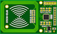
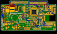
PCB Designer for DC DC Converters Power Supply RFID NFC and Custom PCB Layouts
Need a reliable RF PCB layout or custom NFC and RFID circuit des!gn for your electronic product?
I am David, and I help businesses, startups and product developers turn their electronic concepts into organized PCB des!gns ready for manufacturing.
My services include:
I work with KiCad, Altium Designer, EasyEDA and other relevant des!gn tools to prepare clear, well-organized project files based on your requirements.
Whether you need an RFID antenna circuit, NFC board, wireless communication PCB or custom RF layout, I focus on understanding your project and delivering the files you need.
What you can expect:
Please contact me before ordering so we can discuss your project requirements and choose the right package.