Browse categories
Explore
Fiverr Pro
English
$
USD
PCB Design, Embedded Hardware, Electronics Engineer
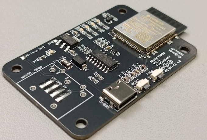
Professional Electronics and Embedded Hardware Design Engineer with 7+ years of experience specializing in high speed pcb design, signal integrity, impedance control. I engineer complex multilayer pcb layouts to guarantee absolute signal validation, pristine data transmission, and strict mitigation of EMI/EMC vulnerabilities.
Services I Offer
Tools I Use
Altium Designer, KiCad, Cadence Allegro, HyperLynx.
File Formats Delivered
Gerber X2, ODB++, BOM, Schematic PDF, STEP 3D Model.
Why Work With Me?

What onboarding documentation is required to initiate the layout process?
To guarantee absolute precision, you must provide your finalized schematic files, component datasheets for custom footprints, and your targeted mechanical enclosure constraints. Clearly defining your layer stackup preferences or target PCB manufacturers early ensures seamless design rule enforcement
How do you handle signal integrity and impedance control setup?
I perform precise trace width and spacing calculations based on your dielectric material constants and layer stackup constraints. This process minimizes reflections and ensures clean differential pair routing for high-speed transmission lines.
Which design environments do you use for high speed pcb design?
Every project is executed natively using industry-standard engineering tools, primarily Altium Designer, Cadence Allegro, or KiCad. This ensures total compatibility with automated fabrication lines and clean export generation.
How do you guarantee the design passes factory fabrication without errors?
Every layout undergoes a rigorous Design for Manufacturing (DFM) and Design for Assembly (DFA) verification loop. I audit track clearances, annular rings, solder mask expansions, and thermal reliefs against real-world manufacturing limits before exporting final files.
What production-ready deliverables are included in the final handoff?
You will receive a complete manufacturing package including production-ready Gerber RS-274X/X2 files, NC Drill files, an IPC-compliant Bill of Materials (BOM), Pick-and-Place coordinates, and a native STEP 3D model.
Can you optimize an existing layout that is failing EMI/EMC compliance?
Yes, I provide comprehensive pcb optimization services to isolate layout bugs, ground plane discontinuities, and signal coupling issues. We will rework trace topologies and power distribution networks to meet standard emission profiles.