Browse categories
English
$
USD
Connect to your AI
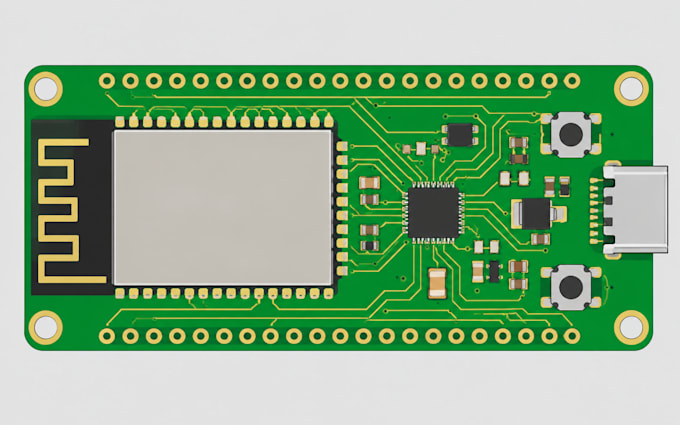
Your ESP32 connects fine on the dev kit, then range drops on your own PCB. That is almost always layout: antenna keep-out, ground plane, or power dips during WiFi transmit.
I design ESP32 (WROOM, S3, C3) BLE and WiFi boards with those details handled from the start:
You receive: schematic (PDF and source), PCB layout, Gerber, drill, BOM, pick-and-place, and a one-page design note covering antenna placement and what to test on your first board.
Not included: firmware, enclosure design, or lab antenna tuning (available as a custom offer).
Before ordering, message me your module or chip, power source and board size limit, and Ill confirm the right package.
Will my board’s WiFi and Bluetooth range match the dev kit?
A: That is the goal of the layout. I follow the module maker’s antenna keep-out and ground rules, route the RF trace at 50 ohms and add a matching network footprint. I can’t promise a specific range in metres, because enclosure and battery
Do you tune the antenna in the lab?
A: No. I design the antenna layout and matching network from the manufacturer’s reference design. Lab tuning with measurement equipment can be arranged as a custom offer.
Which chips do you support?
A: ESP32 (WROOM, WROVER), ESP32-S3 and ESP32-C3 for BLE and WiFi. The Premium package also covers STM32 with an external RF transceiver.
Which chips do you support?
A: ESP32 (WROOM, WROVER), ESP32-S3 and ESP32-C3 for BLE and WiFi. The Premium package also covers STM32 with an external RF transceiver.
Should I use an ESP32 module or the bare chip?
A: In most cases, a module. It comes with a certified antenna and is much simpler and safer for a first board. I’ll recommend the chip-level option only if you need a smaller size or lower unit cost at volume.
Which software do you design in, and do I get the source files?
A: [Your software: KiCad / Altium / EasyEDA]. You receive the full source project, so another engineer can edit it later.
Can you check or fix my existing board?
A: Yes. Send the schematic and layout before ordering and I’ll tell you what I’d change and which package fits.
Can I send the files straight to JLCPCB or PCBWay?
A: Yes. Gerber, drill, BOM and pick-and-place files are included, ready for assembly services.
