Browse categories
Explore
Fiverr Pro
English
$
USD
Expert in electronic and electrical engineering
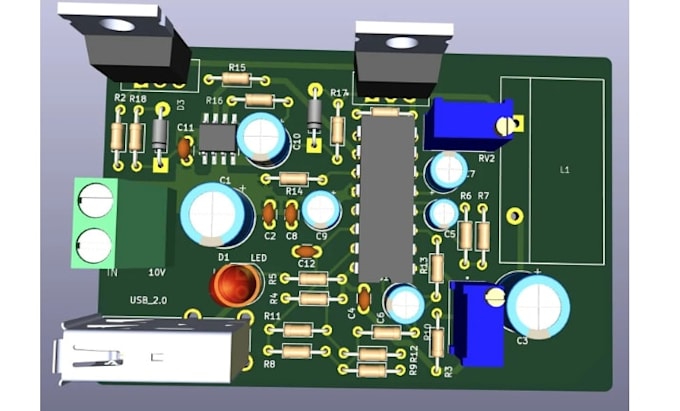
Need a professional PCB design, schematic review, PCB optimization, or PCB routing service in KiCad?
I create reliable, manufacturing ready PCB layouts that improve performance, reduce errors, and ensure efficient production.
I offer
Software & Files:
Perfect for:
Why Choose Me:
Whether you need a new PCB, deslgn optimization, or routing improvements, I deliver accurate and high quality results.
CONTACT ME today and let's build a reliable PCB ready for manufacturing.
Can you optimize an existing PCB design?
Yes. I can improve PCB layout, routing, component placement, power distribution, signal integrity, and manufacturability while maintaining your design requirements.
Can you design a PCB from scratch in KiCad?
Yes. I can design complete schematics, PCB layouts, routing, and manufacturing files based on your requirements.
What does your PCB review include?
My review includes schematic verification, PCB layout analysis, routing inspection, DRC checks, design optimization, and recommendations to improve performance and manufacturing reliability.
Will I receive manufacturing-ready files?
Yes. If required, I can deliver updated design files, Gerber files, BOM, and other production documents ready for fabrication.
Can you fix routing and schematic errors?
Absolutely. I identify design issues and correct routing, connectivity, component placement, and schematic errors to improve overall PCB performance.
Do you review high-speed or multilayer PCBs?
Yes. I can review both simple and complex multilayer PCB designs, including high-speed layouts and IoT hardware projects.
Can you sign an NDA for my project?
Yes. I respect client confidentiality and am happy to sign a Non-Disclosure Agreement before starting your project.
How long does a PCB review take?
Delivery depends on the project's complexity. Simple reviews can be completed quickly, while larger and more complex designs may require additional time.
Why should I review my PCB before manufacturing?
A professional PCB review helps detect design errors early, reduces manufacturing costs, improves reliability, and minimizes the risk of costly board revisions.