Browse categories
Explore
Fiverr Pro
English
$
USD
Your PCB has to survive two things: the signal, and the factory.
I've spent 12 years on both sides. Nine designing PCBs for telecom and industrial equipment that shipped in volume, and three inside SMT and camera-module factories, watching what happens to boards drawn without the assembly process in mind.
WHAT YOU GET
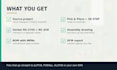
- Complete source project (Altium Designer, KiCad or EasyEDA, your choice)
- Gerber RS-274X and NC drill, verified in a separate viewer before delivery
- BOM with manufacturer part numbers
- Pick and Place file, 3D STEP model, assembly drawing
- Design notes explaining the decisions I made
WHAT I DESIGN
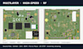
2 to 16 layers. High-speed: DDR3, DDR4, PCIe, Gigabit Ethernet, USB. RF front-ends: VHF/UHF, LNA, matching networks. Switching supplies and PoE. Sensor, IoT and industrial boards.
FILES THAT GO STRAIGHT TO THE FAB
JLCPCB, PCBWay, ALLPCB or your own EMS. No back and forth over broken apertures, missing paste layers or footprints that don't match the reel.
BEFORE YOU ORDER
Send your schematic, block diagram or sketch and I will tell you which package fits and how long it takes. If your project doesn't suit me, I'll say so rather than take the order.


Which files will I receive?
The editable source project plus Gerber RS-274X, NC drill, BOM, Pick and Place and a 3D STEP model. You own all of it. No lock-in.
Can you work in KiCad instead of Altium?
Yes. You get a clean native KiCad project, not an Altium export with broken libraries. EasyEDA as well.
Do you sign an NDA?
Always, before any file is exchanged. Send me yours, or I can provide a standard one.
Can you do the schematic, not just the layout?
Yes. It is included from the Standard package up. On the Basic package, schematic capture is available as an extra.
Will the board actually be manufacturable?
That is the part I care most about. Every design goes through a DFM check against your chosen fab's capabilities before delivery.


