Browse categories
Explore
Fiverr Pro
English
$
USD
PCB Design Engineer Schematic, Layout and Gerber Files
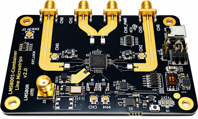
Need a reliable PCB designer for RF, antenna, high-speed, or multilayer circuit boards? I can turn your schematic or concept into a professional, manufacturing-ready design optimized for performance, reliability, and clean layout.
WHAT I OFFER
SOFTWARE I USE
Altium Designer, KiCad, Eagle, EasyEDA, and LTspice.
WHY CHOOSE ME?
BENEFITS
LET'S GET STARTED
Can you design RF and high-frequency PCBs?
Yes. I can design RF and high-frequency PCB layouts with careful component placement, routing, grounding, and impedance considerations based on your specifications.
Do you design multilayer PCBs?
Yes. I can create 4-layer and multilayer PCB layouts with optimized stackups, power distribution, signal routing, and manufacturing-ready files.
Can you integrate an antenna into the PCB?
Yes. I can integrate PCB antennas into your design while considering placement, routing, ground clearance, and your required board dimensions.
Can you handle high-speed signal routing?
Yes. I can optimize high-speed traces with appropriate routing techniques, length matching, differential pairs, and impedance considerations where required.
What PCB design software do you use?
I work with professional tools including Altium Designer, KiCad, Eagle, EasyEDA, and LTspice, depending on the project requirements.
What files will I receive?
Depending on your package, I can provide source design files, Gerber files, drill files, BOM, pick-and-place files, schematics, and other manufacturing outputs.
Can you design from an existing schematic?
Yes. Send me your schematic, component list, board dimensions, layer requirements, and technical specifications, and I can convert it into a professional PCB layout.
Can you work with my existing PCB design?
Yes. I can review, modify, optimize, or complete an existing PCB project. Please send the available files and requirements before ordering so I can assess the work.