Browse categories
Explore
Fiverr Pro
English
$
USD
Electronics Product Development Engineer
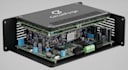
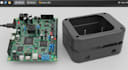
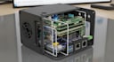
Are you looking for a professional engineer to de-sign PCB boards and custom enclosures for your electronics project? I can help turn your concept into a fully functional and well-structured hardware product.
I specialize in PCB layout de-sign and 3D enclosure development, ensuring that the electronics board and enclosure fit perfectly for real-world use and manufacturing.
Using Altium Designer, KiCad, and Fusion360, I create optimized PCB layouts and precise 3D enclosures suitable for prototyping and production.
My Services Include
Tools I Use
Applications
I focus on accurate PCB de-sign, reliable hardware structure, and professional product enclosure development.
Please contact me before placing an order to discuss your project.
What do you need to start the project?
Please provide project details, circuit requirements, board dimensions, and enclosure preferences.
Which design tools do you use?
I use Altium Designer, KiCad, EasyEDA for PCB design and Fusion360 for enclosure modeling.
Will I receive files for manufacturing?
Yes. You will receive Gerber files, BOM, and 3D enclosure files ready for production.
Can you design the enclosure to perfectly fit the PCB?
Yes. I design the enclosure based on the PCB dimensions to ensure a perfect fit.
Can you help with prototype development?
Yes. I can guide you through PCB fabrication and enclosure prototyping.


