Browse categories
Explore
Fiverr Pro
English
$
USD
Electrical Engineer , Schematic Design , PCB Layout , EasyEDA
I will design clean, professional schematic diagrams and PCB layouts in EasyEDA for your electronics project.
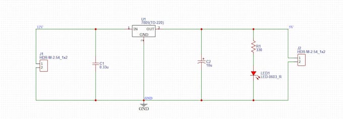
Whether you have a hand-drawn sketch, a rough idea, a PDF, or just a concept I will turn it into a ready-to-use schematic and PCB design.
What you will get:
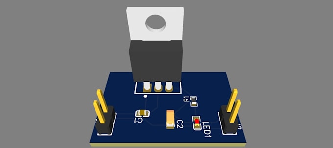
Clean and fully labeled Schematic Capture
PCB Layout (1-layer, 2-layer or multi-layer)
3D View of your board
Bill of Materials (BOM)
Gerber files + Drill files (Fabrication ready)
Source files (EasyEDA)
Perfect for:
Power supplies
Arduino / ESP32 / STM32 projects
Sensor boards
IoT devices
Simple to medium complexity circuits
Converting hand-drawn circuits into professional CAD
Why work with me?
Electrical Engineering graduate
Fast delivery & clear communication
Attention to detail (ERC/DRC checked)
I explain everything simply
Just send me your requirements, sketch, or reference, and I will handle the rest.
Order now and lets bring your circuit to life!


File format:
Gerber
•
STEP
•
VRML
•
SCH
•
Software:
EasyEDA
•
LTspice
•
Matlab
•
Proteus
•
Simulink
•
Arduino
Interface:
HDMI
•
UART
•
USB
•
SPI
•
I2C
•
SDIO
•
Wi-Fi
•
BT
•
Ethernet
What information do you need from me to start?
Please send any sketch, hand drawing, PDF, block diagram, component list, or just describe what the circuit should do. The more details you give, the faster and better I can deliver.
Do you provide Gerber files and BOM?
Yes! In Standard and Premium packages I provide complete Gerber files, drill files, Bill of Materials (BOM), and 3D view so you can directly order the PCB from any manufacturer (JLCPCB, PCBWay, etc.).
Can you work with KiCad or other software?
My main tool is EasyEDA (very fast and free), but I can also work with KiCad, Proteus, and LTspice if needed. Just mention it in the requirements.