Browse categories
Explore
Fiverr Pro
English
$
USD
EMBEDDED SYSTEM AND FIRMWARE DEVELOPMENT
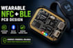
Are looking for a compact and high performance wearable PCB design for your smart device or fitness product? I specialize in custom wearable electronics with BLE, NFC, sensors, and ultra-compact PCB layouts optimized for real-world performance.
I can design complete wearable PCBs using nRF52840, PN532 NFC, motion sensors, barometric sensors, LiPo charging circuits, and BLE communication systems. My designs focus on clean routing, low power consumption, reliable wireless connectivity, and maximum NFC antenna efficiency for wearable applications.
Services include:
Why work with me?
Whether you are building a smart wristband, fitness tracker, or IoT wearable device, I will deliver a reliable and production-ready PCB tailored to your project needs.


What wearable PCB services do you provide?
I design compact wearable PCBs with BLE, NFC, sensors, and power management.
Do you work with nRF52840 modules?
Yes, I specialize in nRF52840-based wearable and BLE hardware designs.
Can you optimize NFC antenna performance?
Yes, NFC antenna tuning and maximum read range optimization are included.
Do you provide manufacturing-ready files?
Yes, I deliver Gerber files, BOM, pick-and-place, and assembly-ready outputs.
Can you design compact multilayer PCBs?
Yes, I create compact and space-optimized PCB layouts for wearable devices.


