Browse categories
Explore
Fiverr Pro
English
$
USD
pcb design
Need a custom FPGA development PCB with reliable power circuitry and high-speed interfaces?
I design FPGA schematics and custom PCB layouts tailored to your hardware requirements.
Your board can include FPGA components, power regulation, clock circuits, connectors, and supported interfaces such as DDR, USB, Ethernet, or PCIe, depending on the selected device and project scope. I consider component placement, multilayer stack-up, routing constraints, and manufacturing requirements during the design process.
Deliverables can include editable schematic and PCB files, Gerber files, drill files, a bill of materials, and pick-and-place data, according to your package.
Please message me before ordering to discuss your FPGA part number, power rails, interface requirements, board dimensions, layer count, preferred design software, and manufacturing needs.

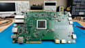
Can you design a custom FPGA development PCB?
Yes, I can design a custom FPGA schematic and PCB layout based on your device and project requirements.
Can you include power management circuitry?
Yes, power regulation and power input circuitry can be included based on the FPGA's voltage and current requirements.
Can you design high-speed interfaces?
Yes, supported interfaces can be incorporated according to the FPGA, routing constraints, and agreed project scope.
Do you support DDR, USB, Ethernet, or PCIe?
These interfaces can be considered where compatible with the selected FPGA and project specifications.
Will I receive manufacturing files?
Agreed deliverables can include Gerbers, drill files, BOM, and pick-and-place data.
Can you design multilayer PCBs?
Yes, layer count and stack-up can be selected based on component density, routing, and signal requirements.
Does your service include manufacturing and testing?
Manufacturing, assembly, and physical testing are excluded unless agreed separately.
