Browse categories
Explore
Fiverr Pro
English
$
USD
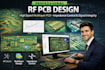
RF PCB Design, High Speed Multilayer PCB, Impedance Control & Signal Integrity
Hi! Thanks for checking my gig. I design high performance RF and high speed PCB systems with a focus on signal integrity, impedance control, and reliable multilayer layouts.
I focus in RF PCB deslgn, high speed PCB layout, impedance controlled routing, and multilayer PCB desgn, ensuring your board performs efficiently .
What I Can Design
What You Will Get
Software
Altium Designer,KiCad,EasyEDA
Applications
LET GET STARTED!

What do you need to start an RF or high speed PCB project?
I need your schematic, stackup (if available), frequency/speed requirements, and design constraints.
Do you design impedance controlled PCBs?
Yes. I design controlled impedance PCB layouts for high speed and RF applications.
Can you handle multilayer and high speed PCB designs?
Yes. I design multilayer PCBs with proper routing, grounding, and signal integrity.
Do you consider signal integrity and EMI in your designs?
Yes. I optimize for signal integrity, noise reduction, and EMI performance.
Will the design be ready for manufacturing?
Yes. You will receive Gerber files, PCB layout, stackup, and documentation ready for fabrication.
