Browse categories
Explore
Fiverr Pro
English
$
USD
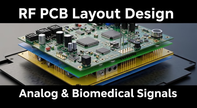
PCB DESIGN
Hello there,
Develop high performance RF PCB layouts tailored for sensitive analog and biomedical signals. This service ensures precise signal integrity, low noise, and optimized routing for high speed, low level biomedical applications. You will receive complete PCB schematics, Gerber files, component placement, and design documentation, ready for fabrication and prototyping. Optional features include multi layer layout, EMI/EMC optimization, and embedded system interface support.
Service i offer
Ready to optimize your biomedical signals? Contact me and bring your PCB to life!


What will I receive with this service?
Complete RF PCB layout optimized for sensitive analog and biomedical signals, including schematics, Gerber files, BOM, and documentation.
Can this PCB handle high-speed and low-noise signals?
Yes, layouts are optimized for high-speed performance, low noise, and EMI/EMC mitigation.
Do you support multi-layer or embedded system integration?
Yes, multi-layer layouts and embedded interface designs are included if needed.
What do you need from me to get started?
Provide target specifications, signal types, number of channels, and any embedded system or component preferences.