Browse categories
Explore
Fiverr Pro
English
$
USD
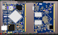
Need a reliable engineer for high-speed PCB design that meets demanding performance requirements? I provide professional PCB layout services for applications where signal quality, impedance control, and routing accuracy are critical.
I design manufacturing-ready circuit boards for startups, hardware companies, researchers, and product developers using industry best practices. Whether your project includes DDR memory, PCIe, USB, HDMI, Ethernet, or other high-speed interfaces, I create clean layouts that minimize noise, reduce crosstalk, and improve overall performance.
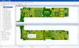
My services include schematic review, multilayer PCB layout, controlled impedance routing, differential pair matching, length tuning, stack-up planning, power distribution optimization, signal integrity considerations, design rule checks (DRC), Gerber generation, BOM preparation, pick-and-place files, and production-ready documentation.
Why choose me?
CONTACT NOW LETS GET YOUR PROJECT STARTED.
What types of high speed PCB designs do you support?
I design high speed PCBs for DDR3, DDR4, DDR5, PCIe, USB 2.0/3.0, HDMI, Ethernet, LVDS, MIPI, SATA, and other high-frequency digital interfaces using industry-standard layout practices.
Which PCB design software do you use?
I primarily work with Altium Designer and KiCad. If your project uses another compatible EDA tool, feel free to contact me before placing an order.
What files will I receive after project completion?
You will receive manufacturing-ready Gerber files, PCB source files, BOM, Pick and Place files, drill files, assembly drawings, and any other deliverables included in your package.
Can you optimize my PCB for signal integrity?
Yes. I apply controlled impedance routing, differential pair matching, length tuning, proper layer stack-up planning, and routing techniques that improve signal integrity and overall board performance.
Can you review and improve an existing PCB layout?
Absolutely. I can analyze your current PCB design, identify routing or layout issues, and optimize it for better electrical performance, manufacturability, and reliability.
Do you design multilayer PCBs?
Yes. I design 2-layer, 4-layer, 6-layer, and higher multilayer PCBs with proper stack-up planning, power distribution, high speed routing, and manufacturing-ready documentation.
What do you need before starting my project?
Please provide your schematic, design requirements, board dimensions, preferred PCB software (if applicable), interface specifications, component list, and any mechanical constraints. If you only have an idea, I can help plan the design from the beginn


