Browse categories
Explore
Fiverr Pro
English
$
USD
Electronics Technician Frontend Developer
PLEASE CONTACT ME BEFORE PLACING AN ORDER
To ensure the best results and confirm project complexity, please drop me a message with your requirements before ordering. Let's make sure we are on the same page!
What I offer in this Gig:
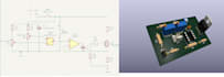
Schematic capture (if you select the extra service)
1 or 2-layer PCB routing and layout optimization
Footprint assignment and custom component creation if needed
Bill of Materials (BOM) with component details
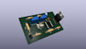
3D model of your finished board (.STEP or 3D view images)
Production-ready Gerber files (compatible with JLCPCB, PCBWay, etc.)
Ideal for:
Arduino, ESP32, and general microcontroller projects
Sensor breakout boards and modular DIY electronics
Student lab projects and small automation circuits
Prototyping and hobbyist designs
My main goal is to deliver clean track routing, proper ground planes, and precise documentation.
Send me a message with your sketch,

File format:
Gerber
•
BRD
•
SCH
•
•
Other
Software:
KiCad
Interface:
UART
•
USB
•
SPI
•
I2C


