Browse categories
English
$
USD
Connect to your AI
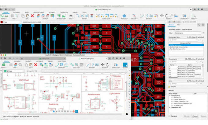
Professional High-Speed PCB Layout Design for DDR, USB, Ethernet, PCIe and Multilayer Boards
Are you developing a high speed electronic product and need a reliable PCB designer who understands signal integrity, controlled impedance routing, and manufacturing requirements? You are in the right place.
I specialize in designing high-speed multilayer PCB layouts for complex digital systems that require stable performance, clean signal transmission, and reliable manufacturability. Whether you are building consumer electronics, industrial equipment, embedded systems, communication devices, networking hardware, or advanced electronic products, I can help transform your schematic into a production-ready PCB layout.
My Services Include:
CONTACT NOW lets get your project started.
What information do you need to start my PCB layout project?
Please provide the schematic, PCB dimensions, layer requirements, component libraries, design constraints, and any specific routing or manufacturing requirements.
Can you design high-speed PCBs with DDR, USB, Ethernet, and PCIe interfaces?
Yes. I specialize in high-speed PCB layout design, including DDR memory routing, USB, Ethernet, PCIe interfaces, differential pairs, and signal integrity considerations.
Which PCB design software do you use?
I primarily work with industry-standard PCB design tools and can deliver files compatible with your preferred workflow and manufacturing requirements.
Will you perform signal integrity considerations during the layout process?
Yes. I follow high-speed PCB design practices such as controlled impedance routing, differential pair matching, length matching, and proper stack-up planning.
What files will I receive after project completion?
Depending on the package selected, you can receive PCB design files, Gerber files, drill files, BOM, assembly files, and manufacturing-ready documentation.
Can you redesign or improve an existing PCB layout?
Yes. I can review, optimize, and redesign existing PCB layouts to improve routing quality, signal integrity, manufacturability, and overall performance.
Should I contact you before placing an order?
Yes. Contacting me before placing an order helps ensure we discuss your requirements, project scope, timeline, and technical constraints for the best possible results.