Browse categories
Explore
Fiverr Pro
English
$
USD
PCB Layouts Circuit Schematics Electronic Design
Are you looking for a clean and professional PCB layout for your electronics project?
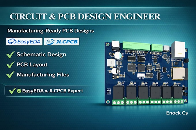
I will design custom PCB layouts using EasyEDA, helping you turn your circuit schematic into an organized printed circuit board ready for manufacturing review.
MY SERVICES INCLUDE:
WHY CHOOSE MY SERVICE?
I focus on clear communication, organized design files, careful routing, and affordable solutions for students, hobbyists, inventors, and small businesses. I will follow your project requirements and provide revisions according to your selected package.
WHAT I NEED FROM YOU:
Please provide your circuit schematic, component list, board dimensions, preferred PCB layers, and any special requirements.
Please contact me before ordering if you need complex designs or additional engineering services.
Let's bring your electronics project to life with a professional PCB layout!