Browse categories
Explore
Fiverr Pro
English
$
USD
PCB Design Engineer, IoT, RF, Reverse Engineering,Gerber, BOM and DFM PCB design
High-speed and RF PCB design problems can quickly turn into costly failures. Many boards suffer from EMI issues, signal loss, unstable performance or complete redesigns after prototyping.
Without proper RF circuit design, controlled impedance routing & signal integrity planning, even a good idea can fail during real-world testing. Issues like poor differential pair routing, wrong stackup design or weak antenna matching often lead to delayed products & wasted development costs.
I will solve this by delivering professional high-speed PCB des!gn, RF PCB layout, rigid-flex PCB design, multilayer PCB routing & HDI PCB development optimized for real performance & manufacturability. I ensure DDR4 routing, EMI/EMC compliance, antenna matching, controlled impedance, signal integrity & power integrity analysis are properly handled from the start.
You get production-ready designs built for advanced electronics, including 5G PCB layout, millimeter-wave RF des!gn, FPGA boards & high-speed embedded systems engineered for stability and reliability.
Whether you need a complex RF circuit, high-speed digital system, or advanced multilayer PCB. Message Me to Get started With your project Now

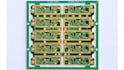
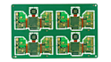
What information do you need to start a high-speed or RF PCB project?
I need your schematic, design requirements, target frequency, layer count, board size, and application details. If you only have a concept, I can help define the RF PCB design, stackup, and layout strategy.
Can you handle RF and antenna design for wireless systems?
Yes, I specialize in RF circuit design, antenna matching, Bluetooth LE PCB antenna design, and 5G millimeter-wave PCB layouts optimized for signal performance and stability.
Do you design for high-speed signals like DDR4 or PCIe?
Yes, I handle high-speed PCB design including DDR4 routing, PCIe Gen 4/5 layout, differential pair routing, controlled impedance, and signal integrity optimization.
Will my PCB meet EMI/EMC and signal integrity requirements?
Yes, I apply EMI/EMC compliant PCB design practices, including proper grounding, stackup design, shielding strategies, and signal integrity checks for reliable performance.
Can you work on complex multilayer or rigid-flex PCB projects?
Absolutely. I design multilayer PCB, HDI PCB, and rigid-flex PCB systems with optimized routing, power integrity, and manufacturing-ready outputs for advanced electronics.


