Browse categories
Explore
Fiverr Pro
English
$
USD
PCB Design Engineer, IoT, RF, Reverse Engineering,Gerber, BOM and DFM PCB design
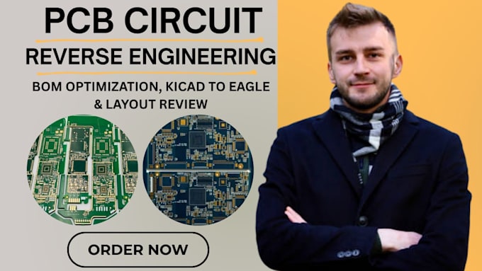
Do you have an old PCB board, missing Gerber files, or outdated electronics that need to be recreated or optimized? Many businesses & hardware developers struggle when original design files are lost, components become obsolete or an existing PCB no longer performs as expected.
Without proper PCB reverse engineering, Gerber recreation, PCB layout review or BOM optimization for manufacturing, you risk delays, expensive redesigns, manufacturing errors & poor product reliability. Incomplete documentation or outdated layouts can make prototyping & production frustrating & costly.
I will help you recover, recreate & optimize your electronics through professional PCB reverse engineering, Gerber reconstruction, BOM optimization, PCB layout review & audit, PCB cost reduction analysis & design for manufacturing (DFM) support. Whether you need KiCad open source PCB design, Altium Designer PCB layout, OrCAD/Allegro PCB layout, Eagle PCB to KiCad conversion, EasyEDA professional PCB design or prototype PCB assembly preparation, your project will be rebuilt with precision & production in mind
Message me before ordering so we can discuss your PCB reverse engineering & optimization Today!!!
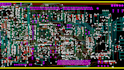
What do you need to start PCB reverse engineering?
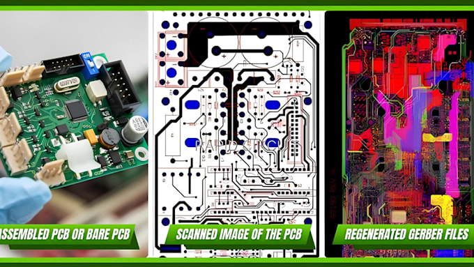
I can work with a physical PCB board, clear PCB images, Gerber files, PDFs, schematics, or existing design files. For PCB reverse engineering and Gerber recreation, the more details you provide, the better the results.
Can you recreate missing Gerber files and schematics?
Yes. I provide PCB reverse engineering, Gerber recreation, PCB layout review, and schematic reconstruction to help recover missing manufacturing files and restore outdated electronics.
Can you convert PCB projects between software?
Absolutely. I support Eagle PCB to KiCad conversion, KiCad open source PCB design, Altium Designer PCB layout, OrCAD/Allegro PCB layout, and EasyEDA professional PCB design workflows.
Can you optimize my PCB for manufacturing and cost?
Yes. I offer BOM optimization for manufacturing, PCB cost reduction analysis, PCB layout review & audit, DFM support, and PCB panelization for production to improve manufacturability and reduce production costs.
Will my PCB be ready for prototyping and production?
Yes. Your files can be prepared for prototype PCB assembly prep, manufacturing support, PCB panelization, and DFM-ready production workflows to ensure smoother fabrication and assembly.