Browse categories
Explore
Fiverr Pro
English
$
USD
PCB Design And Reverse Engineering Expert, KiCad And Altium Designer
Need a professional schematic capture and multilayer PCB deslgn for your electronic project? Im here to help!
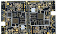
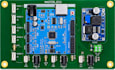
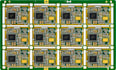
I will create accurate, clean, and manufacturing-ready schematics and PCB layouts using KiCad or Altium Deslgner.
Whether you need a new PCB designed from scratch or an existing deslgn optimized, I can deliver a reliable solution based on your requirements.
My services include:
Schematic capture and circuit design
2, 4 layer PCB design
Component placement and routing
Custom footprints and libraries
Power and ground plane design
DRC, ERC verification
Gerber and drill files
BOM and Pick & Place files
Manufacturing-ready documentation
Editable KiCad,Altium source files
PCB redesign and optimization
I focus on professional layouts, accurate connections, clean routing, and production-ready files.
Send me your schematic, BOM, datasheets, existing PCB files, or project requirements, and Ill turn your concept into a professional PCB design ready for manufacturing.
Contact me today to get started!
What software do you use?
I work with KiCad and Altium Designer for schematic capture and PCB design.
Can you design multilayer PCBs?
Yes. I can design layer PCBs depending on the project's complexity and requirements.
What files will I receive?
Depending on the package, you can receive Gerber, drill, BOM, Pick and Place, schematic, and editable source files.
Can you create the schematic from scratch?
Yes. I can create a complete schematic from your circuit requirements, reference design, datasheets, or existing documentation
Do you provide manufacturing-ready files?
Yes. I can prepare the required production files and perform DRC/ERC checks before delivery.


