Browse categories
Explore
Fiverr Pro
English
$
USD
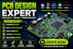
PCB Design and Firmware Development
Hi there,
Need a reliable expert for your PCB design project? I deliver high-quality schematics, PCB layouts, and routing tailored for performance and manufacturability.
What I offer:
Why choose me:
Tools I use:
KiCad, Altium Designer, EasyEDA, DipTrace, OrCAD Cadence
Ready to bring your idea to life?
Send me a message now and let's get started!


What do you need to start my PCB design?
I need your circuit idea, requirements, reference files (if any), and preferred software or standards.
Can you design both schematic and PCB layout?
Yes, I handle complete design from schematic capture to PCB layout and routing.
Do you provide manufacturing files?
Yes, I deliver Gerber, BOM, and Pick & Place files ready for fabrication and assembly.
Can you create custom footprints?
Yes, I can design accurate custom footprints based on your component datasheets.
Which software do you use?
I use KiCad, Altium Designer, EasyEDA, DipTrace, and OrCAD Cadence.
Can you help with complex or multi-layer PCB designs?
Absolutely, I handle multi-layer and advanced routing projects.


