Browse categories
Explore
Fiverr Pro
English
$
USD
CUSTOM PCB DESIGNER
I will design professional PCB layouts, schematics, RF PCB layouts, and automotive PCBs using KiCad.
With 8 years of PCB design experience, I can help turn your circuit idea, schematic, or existing design into a clean and manufacturing ready PCB.
My services include
PCB schematic and editing
2-layer, 4-layer and multilayer PCB layout
RF PCB layout and high-frequency routing
Automotive PCB
CAN Bus PCB layout
Component placement and routing
Power and ground plane design
Footprint creation and verification
DRC and review
BOM preparation
Gerber and drill files
Pick & Place files when required
KiCad source files
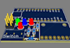
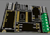
PCB 3D visualization
Existing PCB redesign and optimization
I focus on clean routing, proper component placement, manufacturability, and organized KiCad project files.
Before ordering
Please send your schematic, circuit diagram, component list, board dimensions, required layer count, and any RF, automotive, impedance, or manufacturing requirements.
For complex RF, automotive, multilayer, or high speed projects, please contact me before ordering so I can review the requirements and provide the correct scope.
What do you need from me to start the PCB design?
Please provide your schematic or circuit diagram, component list/BOM, board dimensions, preferred layer count, and any specific PCB, RF, automotive, or manufacturing requirements.
Can you design the schematic as well as the PCB layout?
Yes. I can create or edit the schematic in KiCad and then convert it into a professional PCB layout with proper component placement, routing, power/ground planes, and DRC checks.
Do you design RF and automotive PCBs?
Yes. I can work on RF PCB layouts, automotive electronics, CAN Bus boards, power/control boards, and other specialized PCB designs. Please contact me first for complex projects.
Will I receive manufacturing-ready files?
Yes. Depending on the package, I can provide Gerber files, drill files, BOM, Pick & Place files, and the complete KiCad project/source files.
Can you modify or fix an existing PCB design?
Yes. I can review, modify, optimize, and correct existing KiCad PCB designs or schematics. Send me your current files and requirements so I can review the scope before you order.


