Browse categories
Explore
Fiverr Pro
English
$
USD
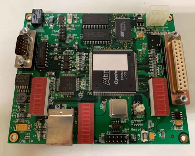
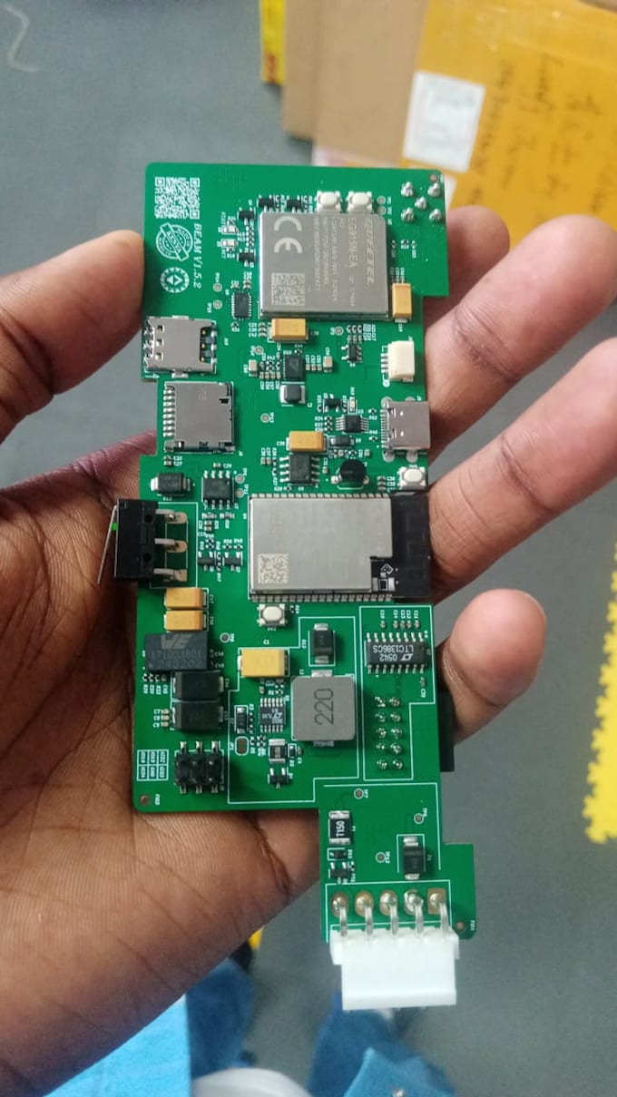
PCB DESIGN LAYOUT ENGINEER
I Offer Professional PCB Layout Design Optimized for Production
Are you looking for a high-quality PCB layout that is clean, reliable, and ready for mass production?
I design professional PCB layouts optimized for:
I'm a trusted and honest Electronics Engineer who specializes in using Kicad as my go-to design tool as it is industry recognized ,however ,if a client requires a specific design tool eg Altium, EasyEDA e.t.c,i can use those too as i am proficient in them. I provide complete end-to-end support from schematic review to fabrication-ready files.
Your files will be ready to send directly to manufacturers such as JLCPCB, PCBWay, OSH Park, or any preferred fabrication house.
Kindly contact me so that we collaborate on bringing your PCB project to life.


File format:
Gerber
•
STEP
•
SCH
•
3DS
•
Software:
EasyEDA
•
KiCad
•
LTspice
•
Proteus
•
AutoCAD
Interface:
HDMI
•
I2S
•
UART
•
USB
•
SPI
•
I2C
•
SDIO
•
Wi-Fi
•
BLE
•
BT
•
GSM/GPRS
•
LTE
Can you design both the schematic and PCB layout?.
Yes, I provide end-to-end design services, including schematic design, PCB layout, and generation of Gerber and BOM files
Can you develop both embedded system firmware and PCB design?
Yes, I can offer a complete solution for PCB design and firmware development. I will need a list of all requirements from you and I will design based on the requirements or even suggest alternatives.
can you write firmware for a PCB Board?
Yes i will provide the most appropriate firmware to run the functionality of your board.