Browse categories
Explore
Fiverr Pro
English
$
USD
Professional Electrical and Electronics Engineer
Need to reverse engineer an existing PCB or recreate a lost schematic?
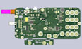
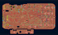
In this gig I'm providing PCB reverse engineering, PCB cloning, PCB redesign, high speed PCB layout, and manufacturing ready Gerber files for reliable reproduction and product improvement.
I help electronics manufacturers, hardware startups, OEMs, repair companies, industrial automation businesses, automotive suppliers, IoT developers, medical device companies, R&D teams, and product developers recover, clone, redesign, and optimize existing PCBs for fabrication and assembly.
Services I Offer
Why Choose Me
Tools
Altium Designer KiCad Cadence OrCAD EasyEDA
Contact Now to discuss your project and receive a professional reverse engineered PCB solution based on your requirements.
What do you need to start reverse engineering my PCB?
I need clear images of both sides of the PCB, schematic (if available), dimensions, and a brief explanation of its function. If you have a physical board, that also works.
Can you recreate a PCB without schematic files?
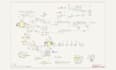
Yes. I can reconstruct the full schematic, analyze the circuit, and recreate the PCB layout even from images or physical boards.
Will the final design be ready for manufacturing?
Yes. You will receive production-ready files including Gerber files, BOM (Bill of Materials), and schematic documentation.
. Can you improve or upgrade my existing PCB design?
Yes. I can optimize your layout for better performance, signal integrity, heat management, or even modernize outdated designs.
Do you handle multilayer and complex PCB designs?
Yes. I work with single layer, multilayer, and high speed PCB designs, including complex routing and signal sensitive circuits.
Which software do you use?
I use professional tools like Altium Designer, KiCad, and EasyEDA depending on project requirements and complexity.
How accurate is reverse engineering from images or scans?
Accuracy depends on image quality and PCB complexity, but I ensure precise reconstruction using circuit analysis and validation techniques.


