Browse categories
Explore
Fiverr Pro
English
$
USD
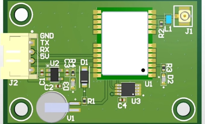
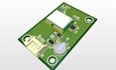
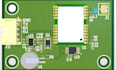
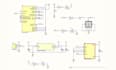
Need advanced multilayer PCB design, PCB layout, and Altium PCB optimized for manufacturing?
Then you've got the right guy for the job. I deliver clean, efficient, and production ready boards with strong performance and reliability using Altium Deslgner, KiCad, and EasyEDA.
I focus on high quality multilayer deslgns with proper routing, signal integrity, and DFM analysis to ensure your PCB works flawlessly and is ready for fabrication.
What I offer:
Software:
Files you will receive:
Benefits:
CONTACT NOW! let's get started.
What details do you need to start my PCB design?
I need your circuit schematic, board size, layer count, component list (BOM), and any specific requirements like impedance control or high speed signals.
Do you design multilayer and high speed PCBs?
Yes. I design multilayer PCBs, including high speed designs with proper routing, grounding, and signal integrity considerations.
What software do you use for PCB design?
I use Altium Designer for professional PCB layout, along with other tools when needed for specific tasks.
Will my PCB be ready for manufacturing?
Yes. You will receive Gerber files, drill files, and fabrication ready outputs optimized with DFM analysis.
Do you perform DFM (Design for Manufacturing) checks?
Yes. I ensure your PCB design passes DFM analysis, reducing manufacturing errors and improving reliability.
Can you improve or optimize an existing PCB layout?
Yes. I can analyze, redesign, and optimize your PCB for better performance, routing, and manufacturability.
Do you handle component placement and routing optimization?
Yes. I provide optimized component placement and clean routing for efficient electrical performance and compact design.
Can you design PCBs for specific applications like IoT or embedded systems?
Yes. I design PCBs for IoT devices, embedded systems, robotics, and electronic products.