Browse categories
Explore
Fiverr Pro
English
$
USD
PCB Design Engineer IoT ESP32 And Embedded Hardware Expert
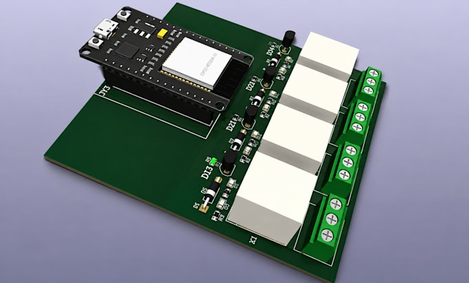
Looking for a professional IoT PCB deslgn, ESP32 PCB deslgn, circuit deslgn, PCB layout, or Gerber file for your electronics project? I will turn your idea, schematic, or technical requirements into a clean, reliable, and manufacturing-ready PCB deslgn.
I specialize in IoT PCB deslgn, ESP32 PCB deslgn, custom PCB deslgn, circuit deslgn, schematic capture, PCB layout, PCB routing, component placement, BOM preparation, and Gerber file generation.
I can deslgn boards for smart devices, sensors, automation systems, embedded systems, wireless products, and other electronic applications.
My service focuses on accurate component placement, optimized PCB routing, proper deslgn rules, clear schematics, and fabrication-ready files.
I can also provide BOM, 3D PCB modeling, source files, and prototype-ready documentation.
Whether you need a simple 2-layer PCB or a more advanced ESP32 IoT board, I deliver professional solutions tailored to your project requirements.
Send me your specifications today and let's bring your electronics idea to life with a dependable PCB deslgn
1. What do you need to start my IoT or ESP32 PCB project?
I need your project requirements, schematic or circuit diagram (if available), component list, dimensions, preferred connectors, and any specific technical requirements. If you only have an idea, message me first so we can discuss the project.
2. Can you design a custom ESP32 PCB?
Yes. I can design custom ESP32 PCBs for IoT devices, sensors, automation, smart products, embedded systems, and other electronics applications.
3. Do you provide the circuit schematic and PCB layout?
Yes. Depending on the selected package, I can provide circuit schematics, component placement, PCB routing, and a complete PCB layout.
4. Will I receive Gerber files for manufacturing?
Yes. I can provide manufacturing-ready Gerber files suitable for PCB fabrication, according to your selected package and project requirements.
5. Can you create the BOM for my PCB?
Yes. A Bill of Materials (BOM) can be included with the Standard and Premium packages or added according to your project requirements.
6. Can you design a 2-layer or multilayer PCB?
Yes. I can design 2-layer and more advanced multilayer PCB layouts based on your circuit complexity, component requirements, and manufacturing specifications.
7. Can you provide the PCB source files?
Yes. Source files can be provided so you can further edit, review, or manufacture the PCB design.
8. Can you create a 3D model of the PCB?
Yes. 3D PCB modeling can be included when required, helping you visualize component placement and board dimensions.
9. Can you work with my existing schematic or PCB design?
Yes. I can work from existing schematics, PCB files, component lists, reference designs, or technical documentation and make the required PCB layout or improvements.
10. Can you handle custom IoT PCB requirements?
Absolutely. Send your requirements before ordering, and I can review your project scope, interfaces, components, board dimensions, and deliverables to determine the best approach.